Navigation
Buffer Circuits
We can now generate sine waves, but our DAC will not let us load the circuit without a significant distortion in the signal. We will see this in action here and build a circuit to prevent this from happening.
DAC waveform distortion under load
Include a diode (red or green) and in series with a 220$\Omega$ resistance at the DAC output. Here are the circuit diagrams for this:
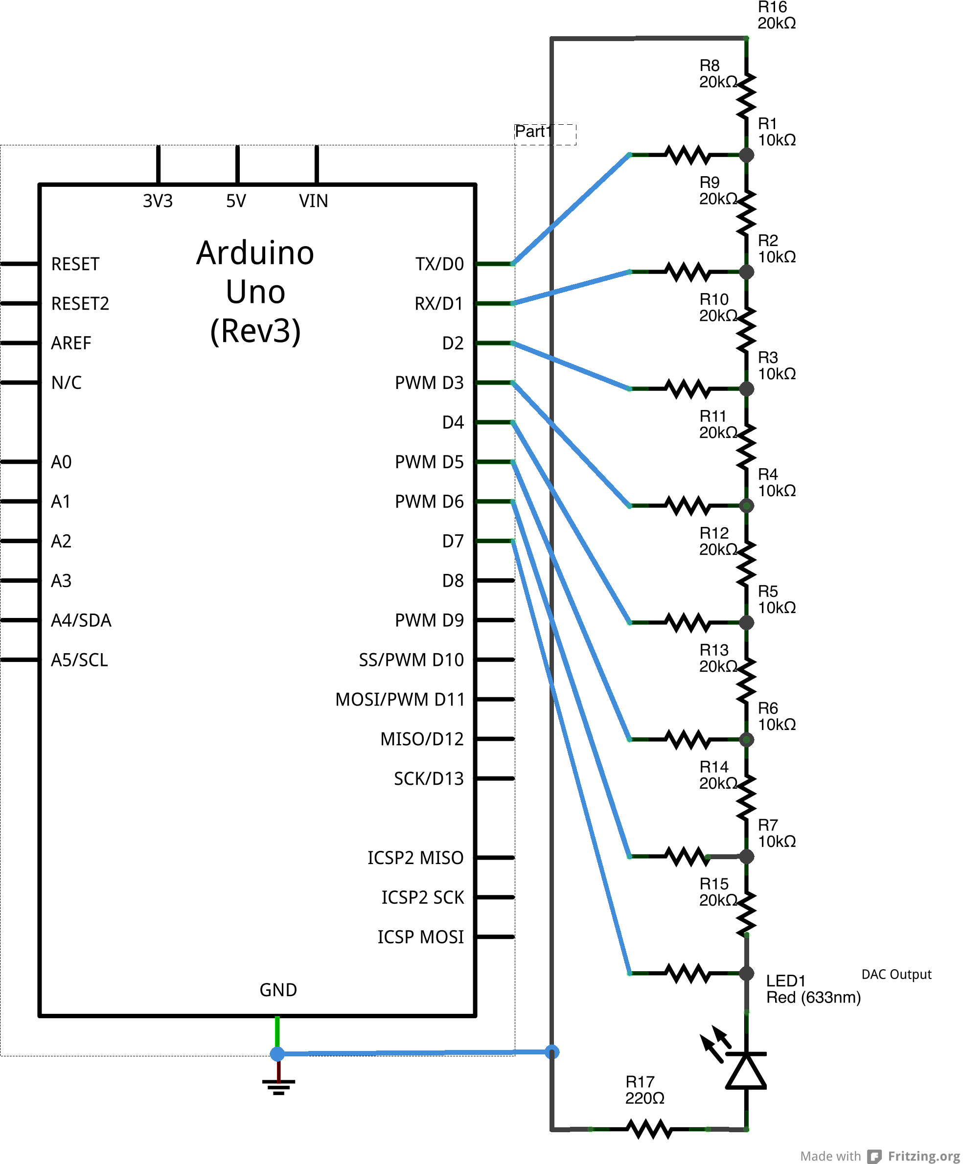
And here is the Fritzing file for the LED circuit.
We need to get the DAC to produce a sine wave and we need to sample it and visualise the waveform. Do this using an oscilloscope. Sample the waveform before you include the LED (which acts as a load) and after you include it. Upload the fast sine wave code for this and ensure that the frequency of the sine wave is around 200 Hz.
Important
Tasks: Sample the sine wave at the DAC output using one of the probes. The other could be placed at ground.
- Does the LED light up?
- What is the shape of the sine wave? It should appear very distorted.
Increase the resistance in series with LED to 10K$\Omega$ or more.
- How does the shape of the sine wave change?
- Make it still larger and monitor the shape of the DAC sine wave.
What do you conclude?
The point here is that the DAC cannot take any load without a distortion in its output. This can be easily seen as follows. From Thevenin's theorem we know that any (linear) circuit with voltages and resistances can be written as an effective voltage and an effective resistance in series. This is illustrated in the following figure:
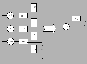
Under load, we have an other resistance in series as follows:

The effective voltage across the load is now
$\begin{equation} V_{\rm out} = I~R_{\rm load} = \frac{V_{\rm eq}}{R_{\rm eq}+R_{\rm load}} R_{\rm load} \end{equation}$
So the smaller $R_{\rm load}$, the more the current flowing in the circuit and hence the smaller the voltage across the load. No longer does the load see the maximum 5V of the DAC output, but it sees something smaller. This is why the sine wave distorts and the peaks get flattened. For a more complete description see the following site from which I have taken the above figures. A PDF file of the site is available here.
We have to find a way of using the DAC without loading it. This is done with a buffer circuit.
Buffer Circuits
A buffer circuit is a unity-gain amplifier that has a (near) infinite input resistance and a (near) zero output resistance. Because of the near-infinite input resistance, $R_{\rm load} = \infty ~ \Omega$ and so, from the above equation, $V_{\rm out} = V_{\rm eq}$. I.e., there is no distortion of the DAC output. Further, because the buffer has is a unity-gain amplifier, the output voltage of the buffer is identical to $V_{\rm eq}$. This is exactly what we want. Buffer amplifiers are represented as:  Here $V_{\rm in}$ is the input voltage (from the DAC) and $V_{\rm out}$ is the output voltage. And $V_{\rm out} = V_{\rm in}$.
We will use an Op-Amp to make the buffer amplifier. You may not know what an op-amp is, but this does not matter. It's full name is //operational amplifier//. These are very high gain amplifiers that can be configured in a number of ways. For this project all we need know is that we can construct a good buffer amplifier out of an op-amp using negative feedback. That is, the output is fed back into the $V_{-}$ input pin of the op-amp. The output of the DAC goes into the $V_{+}$ input pin.
We will use the TS922IN op-amp for this experiment. The biggest advantage of this op-amp is that it can be run off the 5V used by the Arduino. Many other op-amps require operating voltages of 12V which would necessiate the use of an external power supply. The full specifications of the TS922IN can be found here. Please have a look at it as this document contains a lot of important information about this device. The pin layout of the op-amp is as follows:
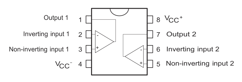
As you can see, there are two op-amps in each package.
What we will do is buffer our DAC output with one of the op-amps in a negative feedback voltage-follower setting, and feed the output of the op-amp to an LED. If all goes well we should then see the LED light level oscillate with the sine wave output of the buffered DAC output. Here is the circuit diagram for this circuit in bread board view (The op-amp is the 8 legged black IC):
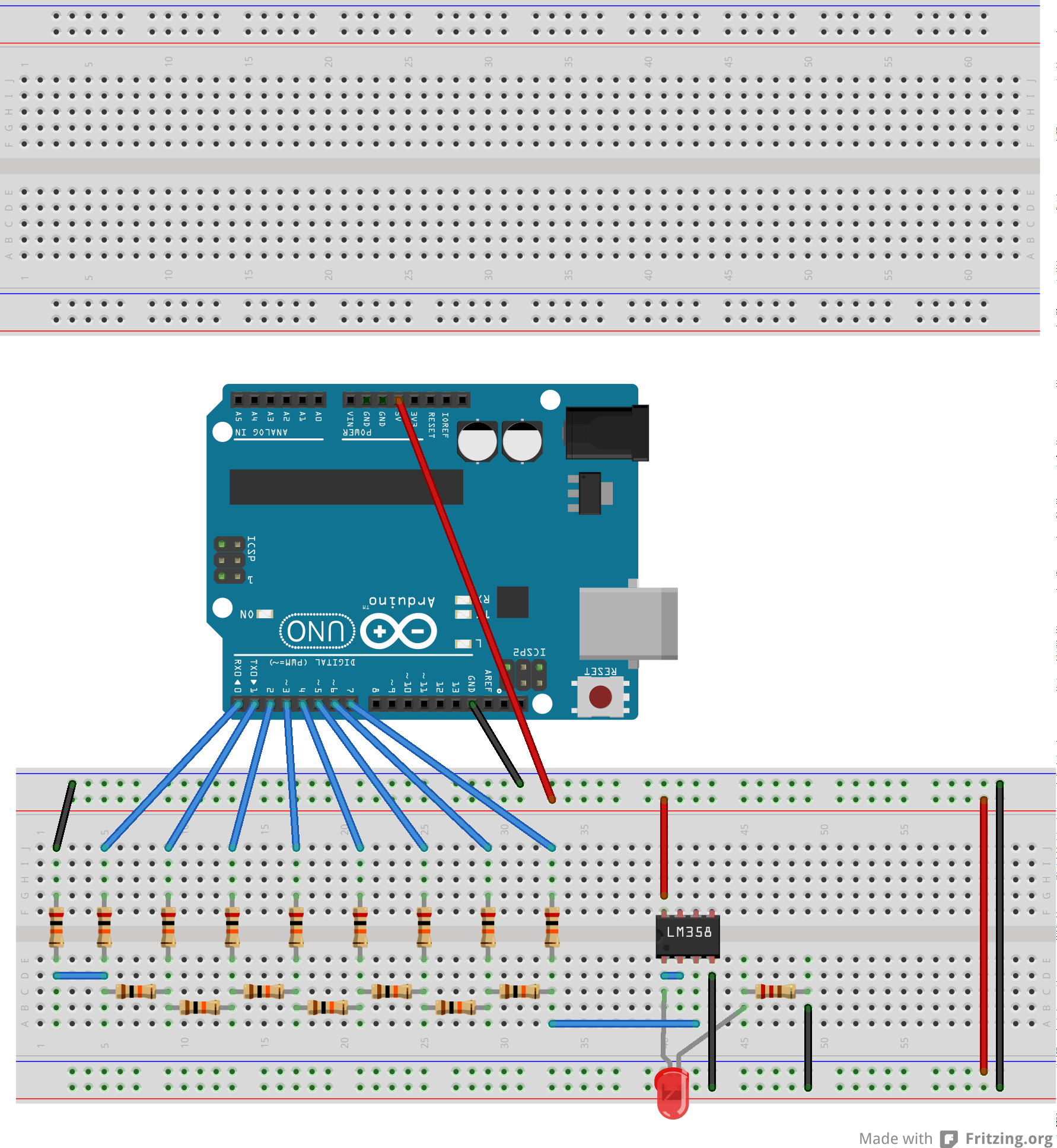
And as a schematic (notice that we do not use the I/O pins of the second op-amp):
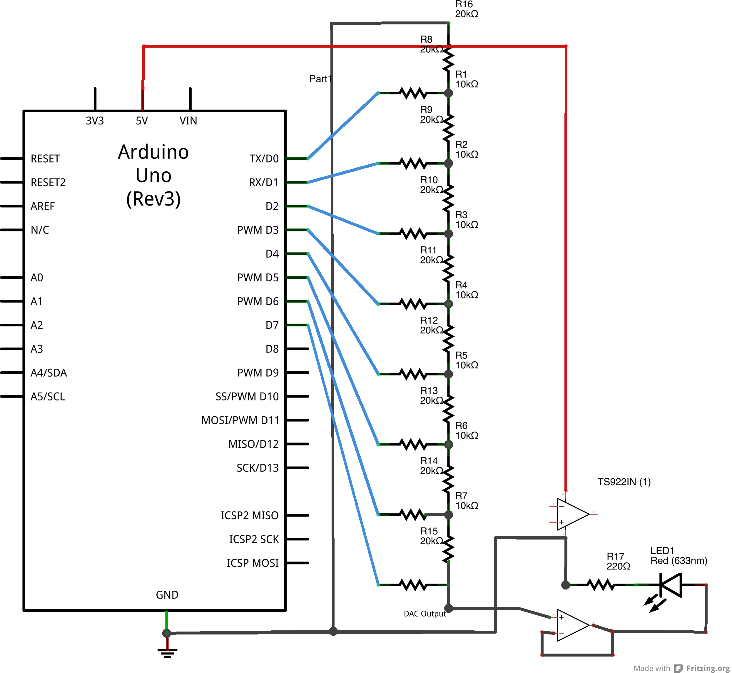
And here is the .
Important
Tasks:
- Use the oscilloscope to view the DAC output before buffering and after buffering. Are they identical? Take a screen shot of the output.
- Explain how buffer circuits work.
We now have a working DAC with an output that can be usefully used. But the output of this DAC is still jagged. It has steps in it and this is not very good for sound generation. The next step in this project is to smoothen out these steps.
